Introduction
Element14 has been running a competition for a DreamBoard and I was wondering how available some of the setups people are requesting are, to work this out I decided to do a simple project. The project goal was to use an ARM processor and incorporate a few sensors and store the data. After looking around I decided to go with the FRDM-KL25Z development board from Freescale and use the FRDM-STBC-AGM01 add on board. As there was no easy way to add an SD card I created my own board for that and at the same time added a battery monitoring circuit to make it a true stand alone unit. All the code was written using mbed to better feature the ARM processor on the FRDM-KL25Z.
Usage Case
The idea behind this project originated from two usage cases with essentially the same basic idea. As I work on equipment that needs to be ruggedized both from the elements as well as from handling, I thought what better way to understand what the equipment goes through than to log it. Its one thing to be told that something needs to stand up to rough handling and abuse but, if that abuse can be quantized it makes designing for the worst case that much easier. The second case and somewhat similar is shipping of fragile packages. It is possible to attach fragile stickers and shock sensitive glass vials but that would only tell you that a threshold force was reached but not for how long or how often or even when during transportation. An active motion logger would resolve all these unanswered questions. Both of these use cases would allow for the use of the FRDM-KL25Z with just one or two add on boards keeping the system simple and as close to a Dreamboard design as possible
Project Goal
Following these two usage cases mentioned above it was important to understand the main goals that this project setou to achieve. As both cases are looking at the handling of an object over a relatively short period of time (1 ~ 8 days) battery life was not critical, a custom battery/SD card board was built but that was mainly because it wasn't until later I found the Freedom Battery Charger Expansion Board. The custom board follows the design of the TI Fuel Gauge BoosterPack but with updated components. Another aspect of the project was price, as it is not known what the units are really exposed to in terms of abuse, keeping the cost low would mean a damaged or destroyed logger would be no real concern in terms of replacement. Along the lines of a damaged or destroyed unit is the issue of data loss, should an event happen to cause a logger to be destroyed that event should, as much as possible, be recorded. Lastly the project should be implemented quickly and kept simple so that any issues that may arise or any requirement changes should be easily dealt with by anyone capable of understanding simple hardware/software.
Data Acquisition and Volume of Data
Looking to log data for 1 ~ 8 days without missing any abusive handling there was a need to establish how fast the system could sample data and store it without losing any of that data. It was decided by a pseudo scientific method that 50 Hz sample rate should be adequate. This was reached by assuming a falling object from one foot or so would take approximately 0.247s to fall, using 50 Hz would give approximately 10 data points on the way down allowing for an approximate drop height to be calculated as well as the force the unit experienced on impact (depending on the surface)
The accelerometer can log data in either 14 bits or 8 bits. Assuming higher resolution and therefore 14 bits that needs 6 bytes of data per sample or 300 bytes per second. The gyroscope also can log data in 8 or 16 bits and again using the higher resolution gives us 300 bytes per second. Since I2C can be set to run at 375 kHz, this would give a data transfer time of ~6.4ms. The I2C bus was eventually set at 400 kHz with a realistic clock frequency of 375 kHz.
Once acquired from the sensors, the data is stored on a SD card for later analysis.The SD card is written too using the SPI protocol which can achieve a theoretical 40 MHz. After some testing it was determined that the realistic speed for the FRDM-KL25Z programed using mbed was only 1 MHz, while very much slower than the 40 MHz desired it posed to be no issue for the setup. Using an 8Gb SD card the unit would be able to log data for ~154 days or well after the batteries are no longer working. This is estimated from 300 bytes/s for each sensor(8Gb / 600 bytes/s / 60s / 60m /24h = 154.32).
The battery life for this project is estimated to be 5 days using a 1200 mAh battery and the full power run current of 7.1 mA for the FRDM-KL25Z, 35 μA for the FXOS8700CQ sampling at 50 Hz and 2.7 mA for the FXAS21002CQR1. This gives a total current consumption of 9.835 mA and for a 1200 mAh battery that gives ~122 hours or ~5 days, if low power mode was implemented for the FRDM-KL25Z this could be further extended. This does not account for SD writes or other components on the boards.
Hardware Setup
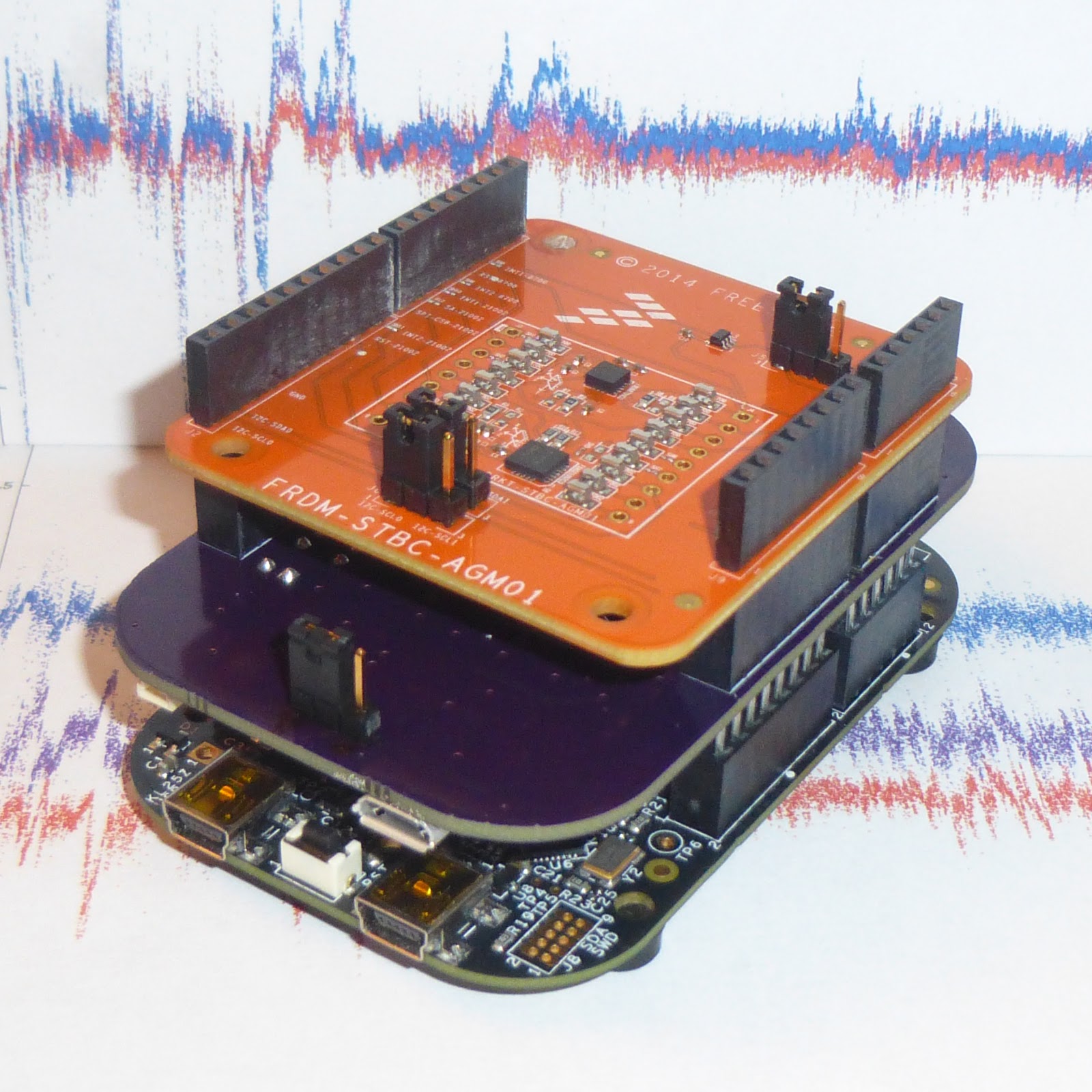
The hardware consists of of three PCBs. The first board is the FRDM-KL25Z that contains the MKL25Z128VLK4 that is the brains behind the system and has the bootloader for the mbed environment.
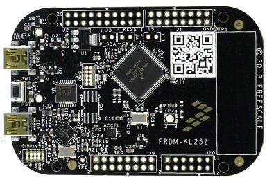
Figure 2. FRDM-KL25Z Development Kit from Freescale
The second board is the FRDM-STBC-AGM01 this board houses the two sensors used in this project, the FXOS8700CQ is a 3 axis accelerometer and magnetometer and the FXAS21002CQR1 is a 3 axis gyroscope. The sensors both use the I2C and SPI protocols to communicate with the host processor. Since there are limited number of SPI modules on the host processor and the data rate of the sensors is relatively low the I2C module was selected. Another reason for this choice is the FRDM-STBC-AGM01 is configured for I2C and the the FXOS8700CQ only works with point to point SPI.

Figure 3. FRDM-STBC-AGM01 Sensor Board from Freescale
The last board is an SD card connector breakout board like the DIGILENT PMODSD PERIPHERAL MODULE or the MIDAS UNO32-SD DAUGHTER BOARD. The board used in setting up this project was a breakout board from 43oh which was replaced by a custom board* that was designed specifically for the FRDM-KL25Z.
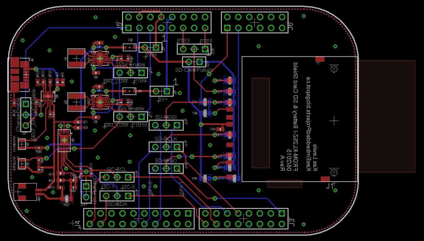
Figure 4. Custom PCB Layout with Space for Both a SD Card & Battery Monitoring
The design of this boards borrows from the TI Fuel Gauge Boosterpack. The circuit is the same except for the BQ27510-G2 which has been upgraded to the G3. While the software for the BQ27510-G3 has not yet implemented when completed this will allow for the system to be truly stand alone and take precautions to ensure all data is saved before the battery is about to die.
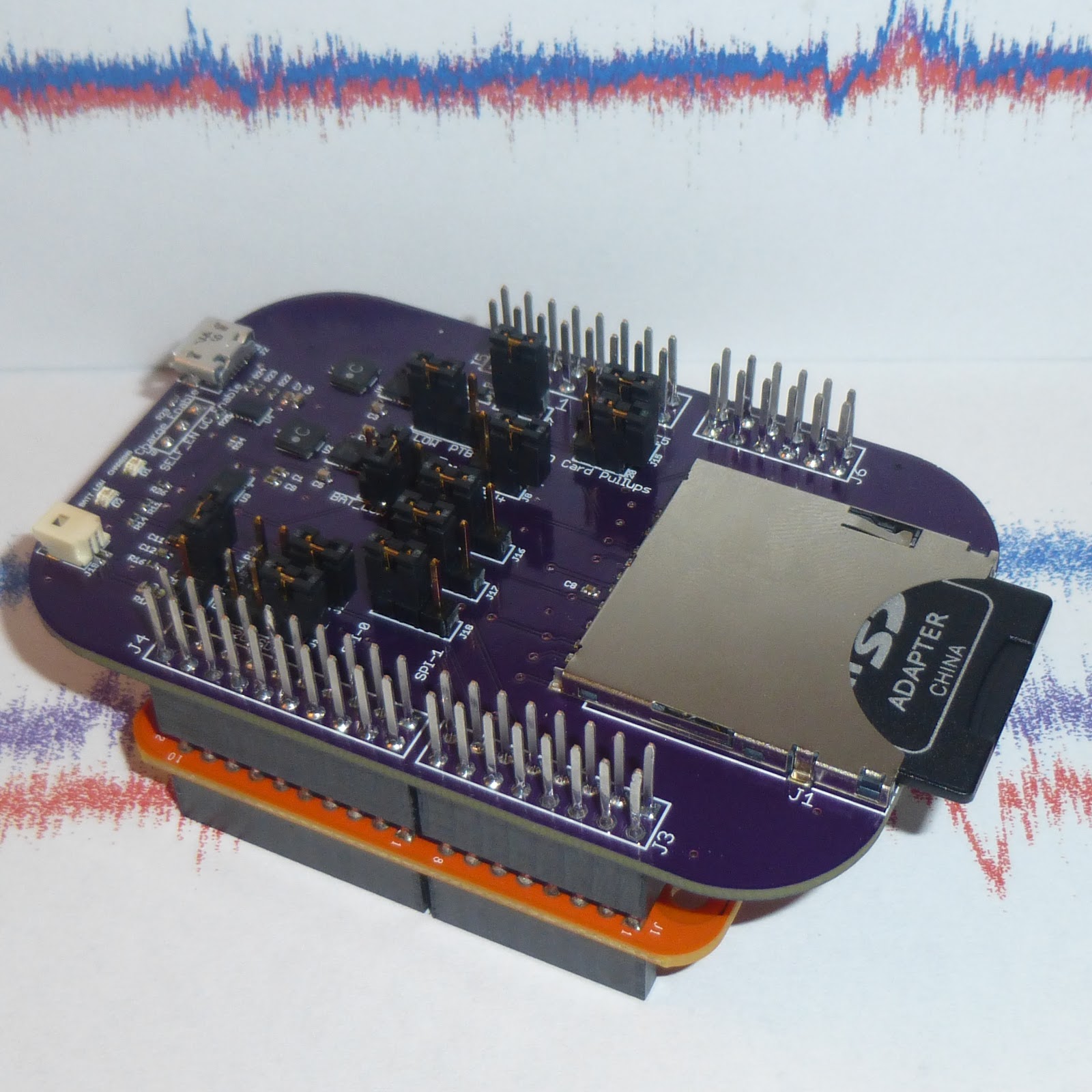
Figure 5. Custom Board with SD Card & Battery Management Circuit
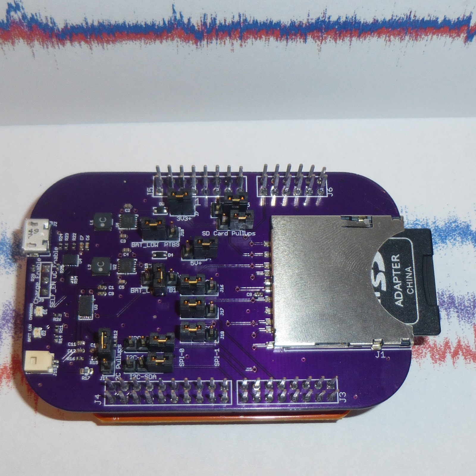
Figure 6. Custom Board with SD Card & Battery Management Circuit
While there is a expansion board from Freescale that has similar abilities, specifically the FRDM-BC3770-EVB, this board does not contain a SD Card slot and this board was only discovered after the custom board had be sent to the fab. The custom board includes both card detect and write protect pins to allowing the host controller to be sure there is an SD card available and in a usable state before starting the system.
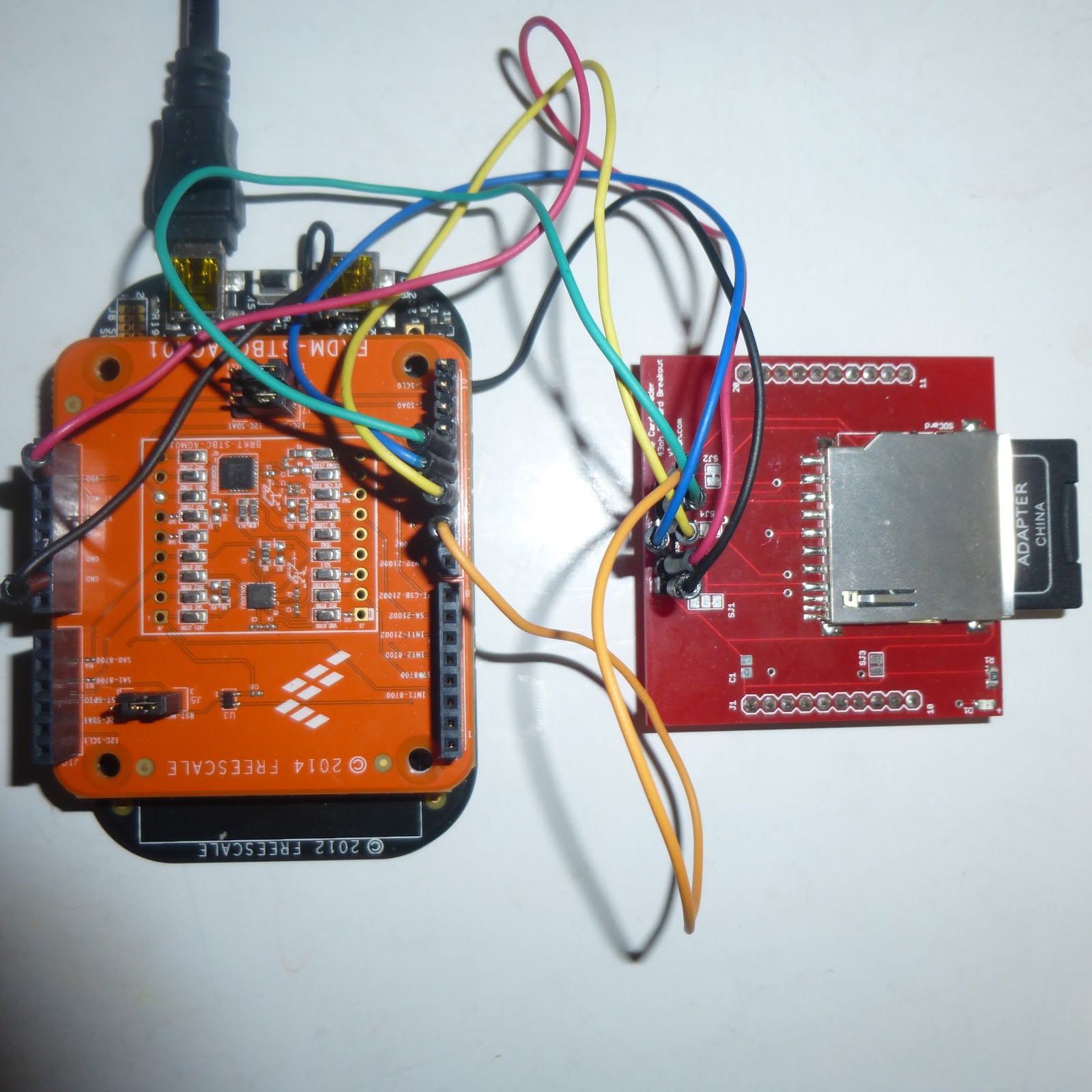
Figure 7. System Implementation Using Three Separate Boards
Software Outline
The software was written in a simple and easy to understand style to allow for anyone wanting to read over the or modify the code to be able to do so. For this reason the code follows a very simple progression as will be outlined below. The code was written in the mbed environment allowing for further simplification, at each stage in the flow diagram for the software there is some code that demonstrates what is required at that stage of the software flow. The full program can be found in the mbed repository here.
This project uses interrupt driven programming, this means that all events in the main loop only happen after an interrupt routine has set a flag signaling for the main loop to take action. Both interrupts that are used are fired when a sensors has recorded a preset number of samples in its FIFOs. When the interrupt occurs it sets a flag letting the mainloop know that there is data to be fetched from that sensors FIFO.
Figure 8. Interrupts That Drive the System
The first step in the code is to include the two libraries that are needed, mbed.h adds the basic functionality for the chosen platform and SDFileSystem adds the functionality for writing data to the connected Sd card. Once the needed libraries have been added, the registers used by both the FXOS and FXAS sensors are defined, this allows us to keep later I2C calls simple and self explanatory. The next step is to initialize the needed system modules.
Looking at the flowchart below we see the first module that is initialized is the serial port. This port is mainly used for debugging as it is a relatively slow port and in mbed serial communication is a blocking operation, it is therefore not desirable to use the serial port during high speed data acquisition. I2C is initialized to enable communication with the sensors and at a later stage the battery monitoring IC as well. The I2C port used is port PTE pin 0 for the data line (SDA) and pin 1 for the the clock (SCL).
Setting up the interrupts is a two step process, first we set pins to be interrupts in this project, pins PTD4 and PTA5 are set as FIFO full interrupts from the two sensors. The second step with regards to interrupts is done in the main function and that is to assign what to interrupt on (high -> low or low -> high transitions) and when an interrupt occurs what function should be called. In this case both interrupts are happen on a rising edge and they call functions called fxas_data and fxos_data respectively.
The last step in the initialization before going into the main function is to set up the Sd card communication. This is done by creating a SDFileSystem object and then giving that object the pins used for MOSI, MISO, SCLK and CS. In this project the default SPI port was used, PTD2, PTD3, PTD1 and PTD0 respectively. It has been verified that it is possible to use other SPI ports but for simplicity only one is pointed out on the platform pin descriptions.
After the initializations are completed the I2C clock frequency and serial baud rate are increased to allow for faster communications and reduced interruptions. For this reason the SDFileSystem used in this project has been modified to increase the clock frequency to 1 MHz to prevent the system from losing data during a SD card write cycle. The next step is to create a directory on the SD card in which to place or data and a file with heading. The last step in the main functions initializations is to set up and start the sensors, this is done by calling fxas_init() and fxos_init(). Once all these steps have been completed the system will start logging data.

Figure 9. System Initialization
The main loop runs in the background and does all the heavy lifting. The first step in the main loop is to look for a FIFO full flag set in one of the two interrupts. Once a flag has been set the main loop will read all available data samples and store them in a local buffer. This buffer was arbitrarily set at 23, for better performance and possibly longer sleep times by the processor this could be set to 30 or 32 samples. When all the samples have been read from the sensor a data ready flag is set, this flag indicates to the next step of the main loop that data is ready to be sent to the SD card.
After data from both sensors has been read in, which should happen very close in time as both sensors are running at 50Hz, the main loop will send all available samples to the SD card. To do this correctly and in somewhat of a understandable fashion the MSB and LSB of each sample are concatenated before sending the data to the SD card. As the accelerometer data is 14 bits long and the LSB is left justified, there is a need to first shift the MSB left by 8 bits then OR the two bytes and finally right shift all 16 bits by two to arrive at 14 bits of data. As fractional operations are computationally heavy on microprocessors multiplying the data by either 0.976mg or 7.8125mdps has been left to be completed on the PC.
Once all data has been sent to the SD card the file is closed, this is done once every 30 cycles to ensure minimal amounts of data are lost. It is not done more frequently as this adds extra overhead to the SD write cycle. After closing the file the buffers are cleared, while not essential this was done to remove any question as to the correctness of the sampled data.
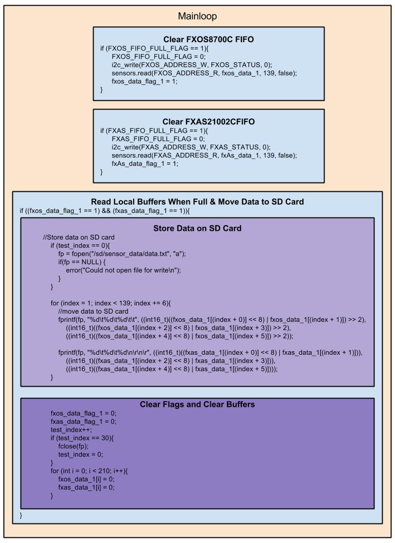
Figure 10. Main Loop Where the Time Consuming Operations Occur
The software in its entirety can be found here, the project can be added to your project space and then downloaded to your own FRDM-KL25Z from that location.
MBED
As part of this project was to show of the ARM core at the center of all the processing, the mbed environment was used. Along with showing of the ARM core mbed also allows for implementing programs in relatively simple and quick ways to be used as a prototype or in some circumstances for get to the final product quickly. While using mbed for this project I realized the ease with which other wise long and complex tasks can be achieved. Setting up interrupts and along with what action should be taken when fired only takes two lines. Similarly setting up the SD file system also takes two lines of code.
That being said there are some thing to watch out for. During this project I was not able to use the blue LED for debugging, this was discovered only after I was no longer able to save data to the SD card. It was later noticed that the SD card clock and the blue LED are on the same pin. Other issues where setting clock frequencies. The clock for the SPI but does not appear to be able to be set above 1 MHz, while I have tried a few different ways to reach this I was not able to do so. The same issue is noticed with the I2C bus, going above 375 kHz does not appear possible, I was hoping to achieve 400 kHz but setting the frequency higher only seems to decrease the clock frequency after a certain point.
Also not having a built in debugger when you are used to depending on one is a huge change in the game. Another big change that may take getting used to is the bootloader. Where with a conventional IDE there is a one step compile and program, here there is a two step compile and download and then drag and drop into the platform. While not a huge game changer it does slow down the programing iterations. Both of these may have bothered me but in a weird way I feel doing more programing like this would make you a better programmer as there is a need to do this better and in a more thought out manner the first time and less by trial and error.
With a few issues encountered along the way there is one very big positive to mbed. There is a large and very helpful community. No matter how big, small or subtle the issue I found that the community was both willing and very capable of helping.
Project Testing and Usage
The project while on a basic level is complete this is room for further progress. At this point there is a need to use the project to log how a package that is shipped is handled so as to better understand the design constraints to build a resilient outer shell.
In order to use this unit in a somewhat meaningful way the data obtained from this project is put through a graphing program to determine how the unit has handled. My program of choice is GNUPlot or Excel. While Excel has a limitation on the number of points it will plot for you (1048576) GNUPlot does not. Below I have included data samples from some test with this project to give an idea of what the project is capable of.
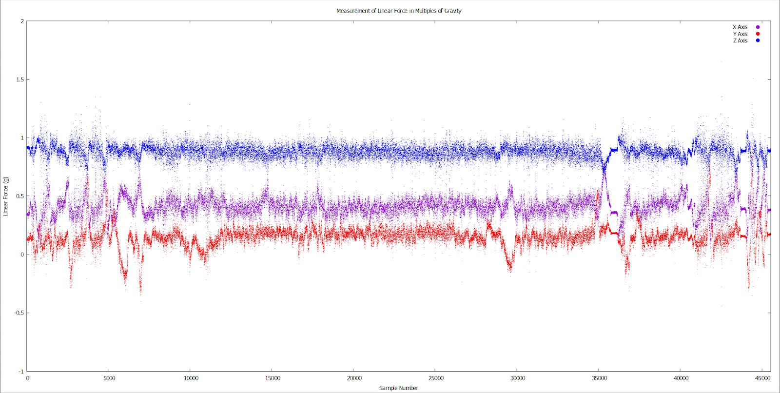
Figure 11. Accelerometer Data Recorded on a 15 Minute Drive
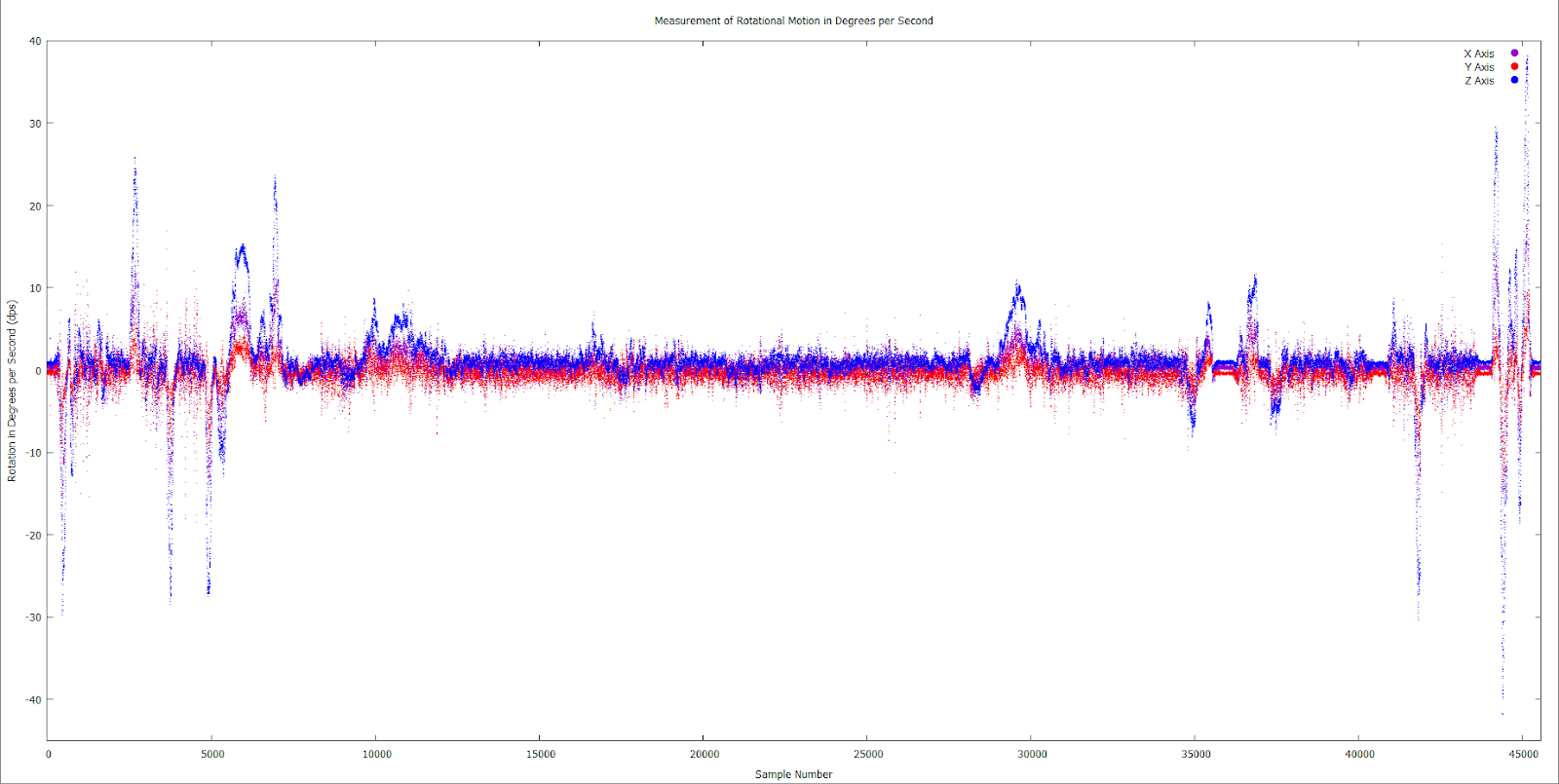
Figure 12. Gyroscope Data Recorded on a 15 Minute Drive
Issues experienced and their resolutions