This Time
In this blog post I plan to go over the board layout for the components chosen in the previous blog entry and explain the reason for the layout and placements that I have chosen. I was hoping to give an outline for the software but due to the stage in the design that will have to wait.

Figure 1. Almost Complete Board (No power routing)
Layout
I designed and laid out the board using Eagle and for this design I opted to make most of the schematic symbols and footprints. I felt it would give me better knowledge of what was happening in the design. While this does take more time (especially when you read the data sheet incorrectly) it did help me have a better understanding of how to orientate components when working on the PCB layout. The main drive behind the layout was to reduce cross talk between signal traces and to have the smallest form factor. The first drive follows a recent seminar I attended in which the main message was, all traces should be treated as transmission lines and as much as possible all traces should be one dielectric from ground. After looking around, this simple message of “one dielectric from ground” is a very big and complex topic one that maybe in a future blog I will attempt to tackle.
In working with the second drive, component placement became a big issue and in this application there were two considerations. The first has to do with the type of sensors being used. There are three magnetometers (LSM9DS0, LSM303D, MAG3110) and according to Freescale’s app note, magnetometers should be placed as far as possible from signal and high current traces (due to electric currents producing magnetic fields). With this in mind a lot of time was spent trying to keep the three magnetometers somewhat isolated.

Figure 2. Magnetometers (yellow) separated from other components
The second consideration with placement and in some ways a conflicting requirement was to have a balanced PCB. Since the rocket will not be much larger than the PCB there is a concern that an uneven horizontal distribution may cause the rocket to be unstable. (Note: the physics have not been worked out nor is it known how fast the rocket rotates if at all wich may render this concern moot).
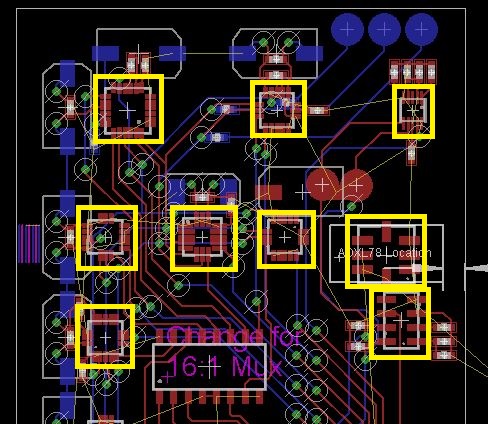
Figure 3. Attempting to balance the board to prevent the rocket from wobbling
As I am still in the layout phase, I will explain how the layout reached where it currently is and hopefully point out a few things I learnt along the way. It can be daunting opening the PCB layout after completing the schematic design.
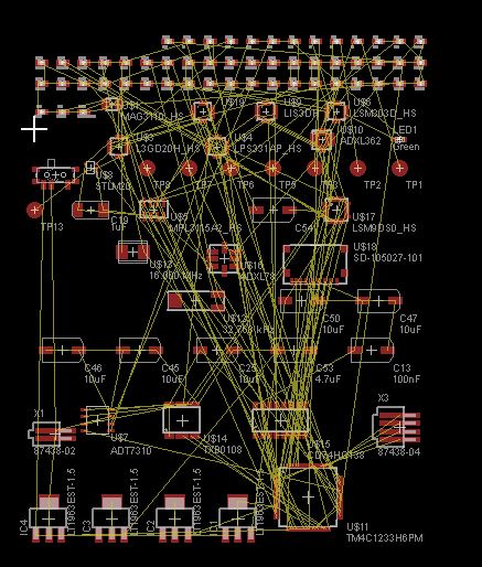
Figure 4. PCB Layout after completing schematic
After going through countless sites, not one listed a good way to start your layout for anything more complex than four or five components. After trying various techniques the one that worked best was to group all main components (sensors, uC, etc.) with their secondary components (resistors, capacitors, etc) and then work with the groups. Once everything is grouped, moving the groups to reduce the number of crossing air wires between major components helps reduce later frustration. One very obvious but probably overlooked option is to move connections from one pin to another. Doing this may be some what tedious but in terms of layout and preventing traces from crossing eachother or needlessly being routed halfway around the board, this can make the final layout a lot simpler and cleaner. In my design I moved connections around multiple times helping to reduce the need for vias and potential cross talk.
Once major components are arranged the secondary components need to moved to ensure they are where they need to be relative to the major component (some capacitors need to be connected to a specific pin, read the data sheets). Once secondary placement is completed anything that is left can be arranged to decrease crossing airwires. This whole process is an iterative process. For the current design, I have already done numerous times.
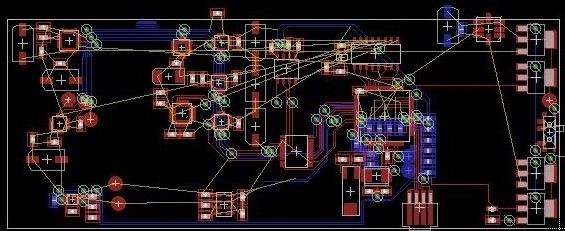
Figure 5. Original PCB layout proposed
Once component placement is complete everything needs to be connected. At this point the “one dielectric from ground rule” applies. Ensuring anything that has fast switching speeds (not clock speeds but transistor switching speeds) is closely coupled to ground can be a mission in itself. A lot of time was spent ensuring as many signal lines as possible were closely coupled to ground to reduce any chance of cross talk or coupling between single lines. During this stage I still continued to move component groups and even swapping pin connections to achieve simpler routing. At times the simplest method to see how the routing would work was to route the connections and use the move tool to see how that trace could be best arranged. It may not be evident for the pictures but I have allowed enough space for the ground plane to fill most of the spaces between signal traces.
This may not always be easy but seeing as data transmission rates are increasing as are transistor switching speeds (this is one of the main causes for noise) if we don’t start now it will only be harder later.
One thing I did not mention was in the design phase I tried to always keep power sources as close to where it would be needed in a hurry. This is accomplished by putting bulk capacitors close to all sensors (yes this is in most reference designs) but not just for Vcc, if there is another power line that may have a sudden power draw, I have put one there as well. Keeping rapid long distance power demands low (using a local pool and letting that replenish slowly over time) helps to keep fluctuations on traces low decreasing noise. Along with each bulk capacitor there is a decoupling capacitor to reduce line noise.
Over all I have spent a few weeks getting to where I am now starting from a very general layout to moving each component group and switching pin connections as needed to finally having a layout that I am almost ready to have fabricated.
Hopefully all connections and footprints are correct and I will have a workable board first time round (really hoping)
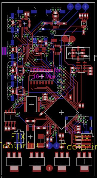
Figure 6. Bigger view of current board
No comments:
Post a Comment